| Label | Original Part | Replacement Part | Cost |
|---|---|---|---|
| CR8 | N/A | On Semiconductor BZX84C2V4LT1G |
$0.14 |
| U1 | Supertex HV518PJ |
Microchip HV518PJ |
$5.52 |
| U7 | Intel N80C51BH |
Atmel AT89S51 |
$2.01 |
| U9 (VFD) | Samsung SVI-12MS06 |
Shanghai Pufeng Opto Technology SVI-12MS06 |
N/A |
| U11 | NEC uPD43256BGU-70LL |
NEC uPD43256BGU-70LL |
$2.46 |
| U12 | AMD AM27C020-150JC |
Atmel AT27C020-55JU |
$2.57 |
| U16 | National SCX6206AK0 |
National SCX6206AK0 |
$12.31 |
| U17 | Intel N80C196KB16 |
Intel N80C196KB16 |
$3.08 |
| U34 | Analog Devices AD586KRZ |
Analog Devices AD586KRZ |
$9.83 |
| U138 | On Semiconductor MC3423D |
On Semiconductor MC3423D |
$1.54 |
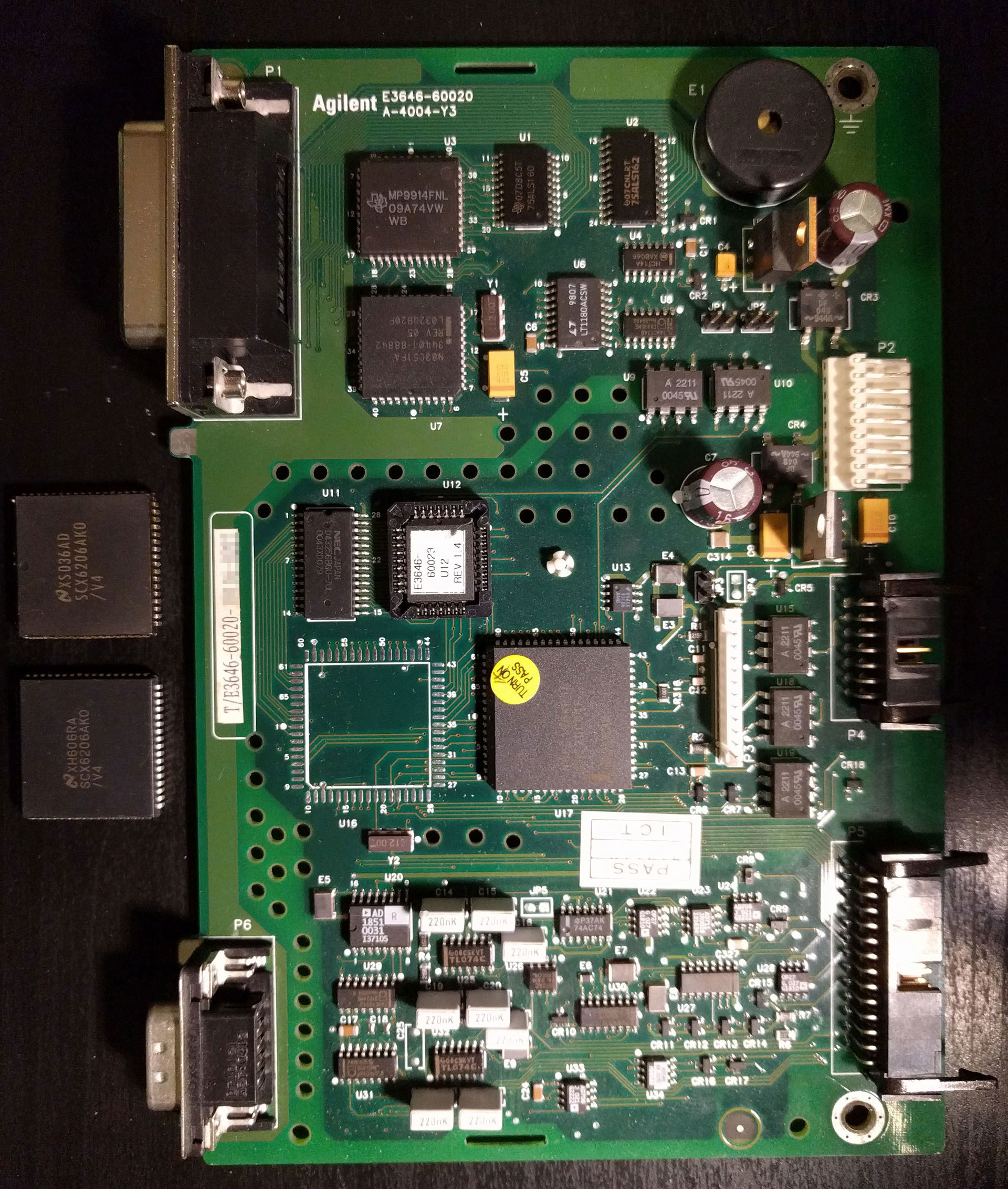
Back in January 2017, I picked up a broken Agilent E3646A bench power supply. When it was turned on, all of the segments on the vacuum fluorescent display (VFD) would light up, the unit would quickly beep twice, then the VFD would go blank and the unit became unresponsive. According to the user manual, this corresponded to error 601, which meant that U16 (National SCX6206AK0) on the control board could not communicate with U7 (Intel N80C51BH) on the display board. Given this diagnostic information, repairing the unit initially seemed fairly straightforward.
Problem #1: Blank Display
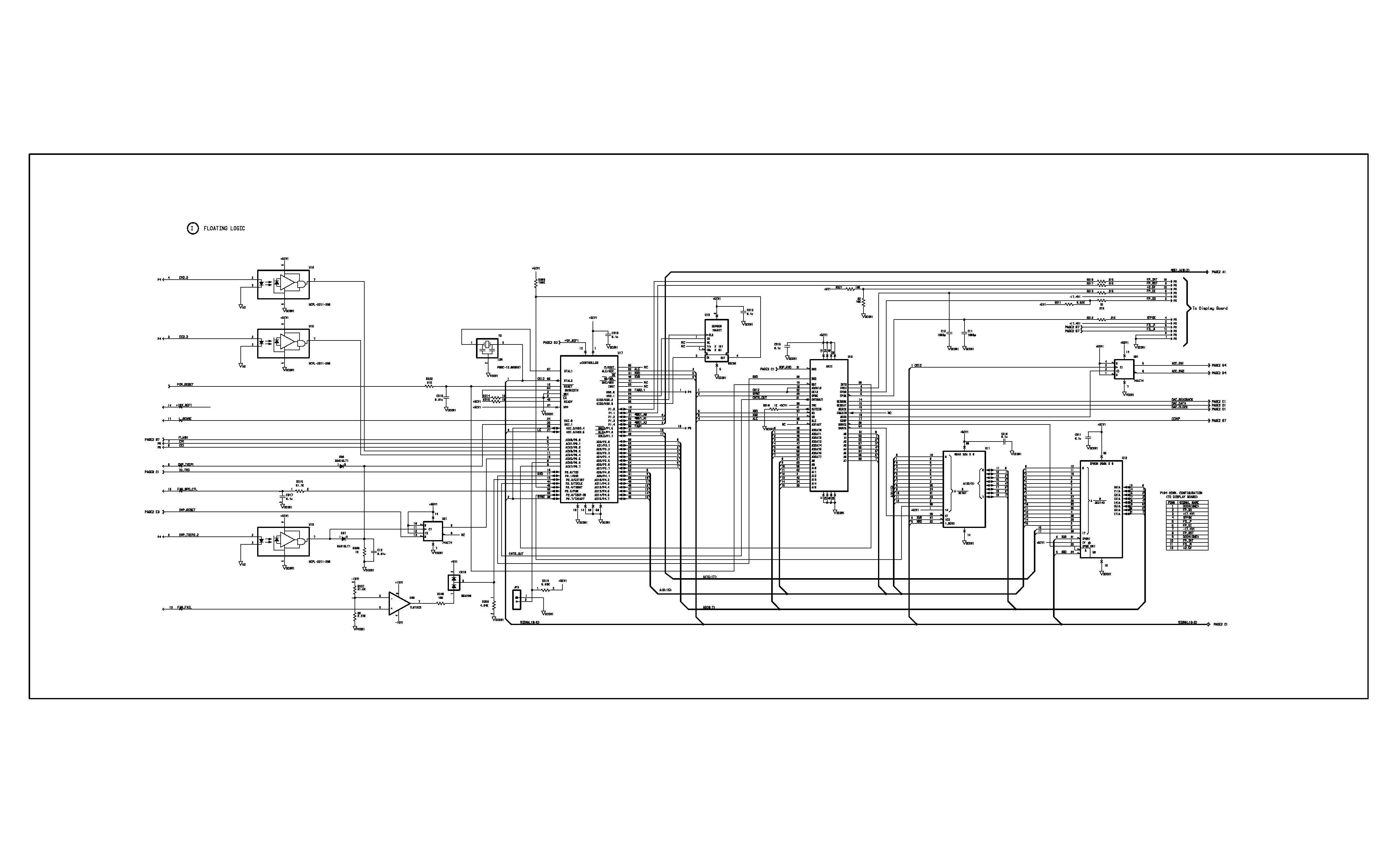
Control board schematics, extracted from service manual pg. 216
On the control board, I checked the FP_DI (data in), FP_DO (data out), FP_SCK (clock), FP_INT (interrupt), and FP_RST (reset) traces from gate array U16 and microcontroller U17 (Intel N80C196KB16) to the cable assembly, and through the wire harness, which all tested fine. Next, I disassembled the display board, but discovered that the physical layout of the board meant I would need to remove the VFD in order to access the circuitry behind it. This proved to be much trickier than I expected, especially with only a temperature-controlled iron and desoldering wick, but it worked out.
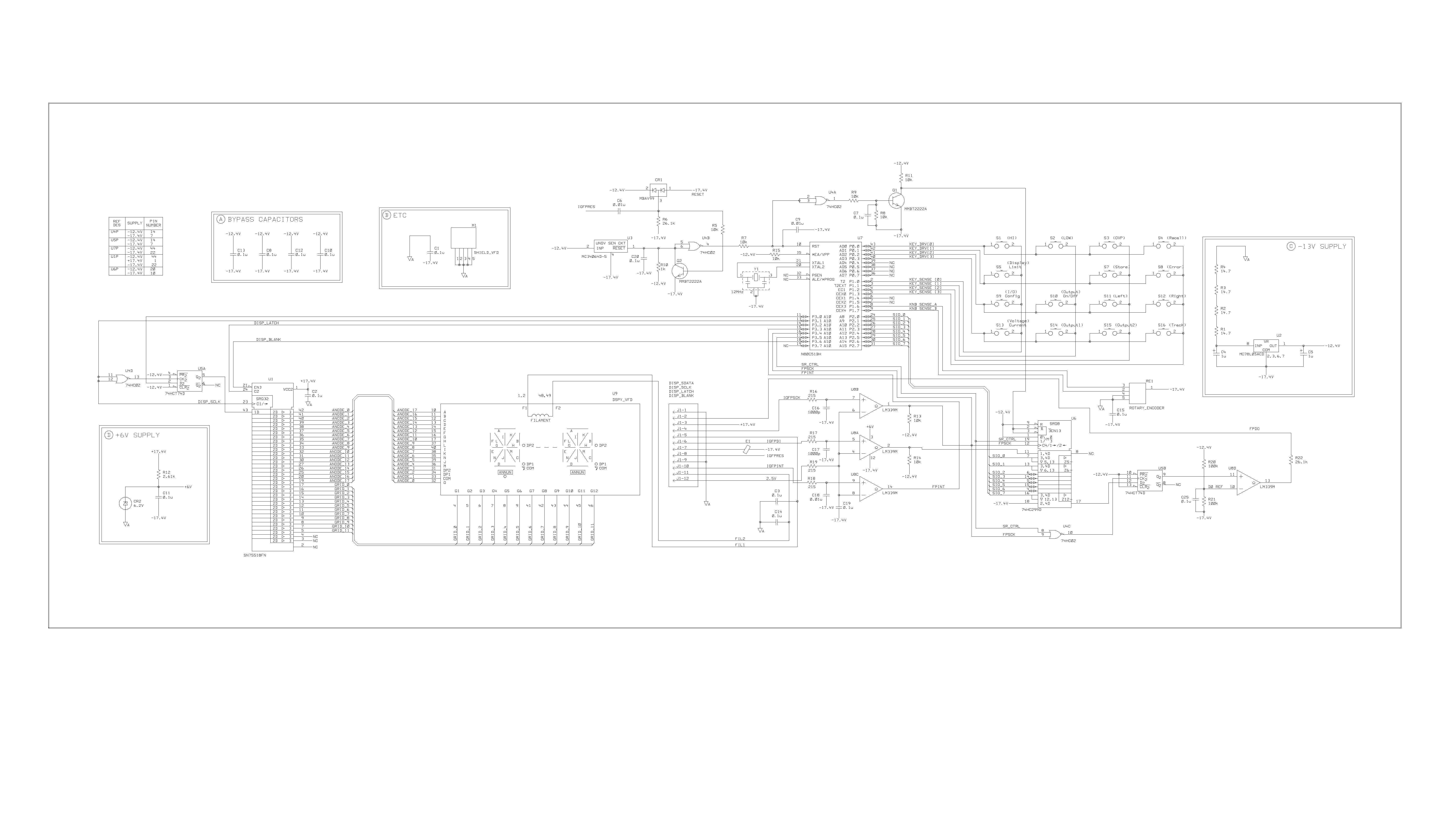
Display board schematics, extracted from service manual pg. 218
Next, I followed these traces from connector J1 through the quad comparator U8 (National LM339M), shift register U6 (Philips 74HC299), dual flip-flop U5 (Philips 74HCT74D), and quad NOR gate U4 (Philips 74HC02), probing with my Saleae Logic 8 logic analyzer. Note that only a +17.4V, -17.4V rail, and a +2.5V reference are supplied to the display board, so linear regulator U2 (National LM78L05ACM) and reverse-biased zener CR2 provide a virtual +5V rail (absolute -12.4V) and an absolute +6V rail, respectively. As a result, the 2.5V reference and comparator U8 effectively serve as a level shifter for the input FP_SCK, FP_DI, and FP_INT signals from the control board to the display board, which then clock and feed into the shift register U6, which can be read by the microcontroller U7. The output FP_DO signal follows a similar circuit in reverse; it is written by the microcontroller U7 to the shift register U6, clocked into the flip-flop U5 by the clock control NOR gate U4, and level shifted by the remaining comparator in U8. Two 100k resistors, R20 and R21, form a voltage divider with +2.5V virtual (-14.9V absolute) output for the inverting input. But since the comparator U8 operates at +23.4V rail-to-rail (+6V to -17.4V), another level shifter on the control board converts this back using a voltage divider formed from the 215 Ohm resistor R1 and 5.62k resistor R311 biased to +5V.
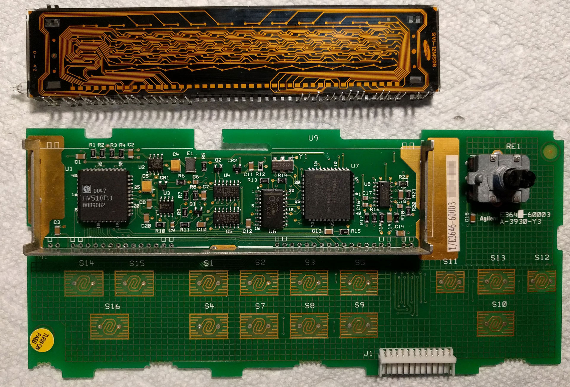
Original display board, disassembled
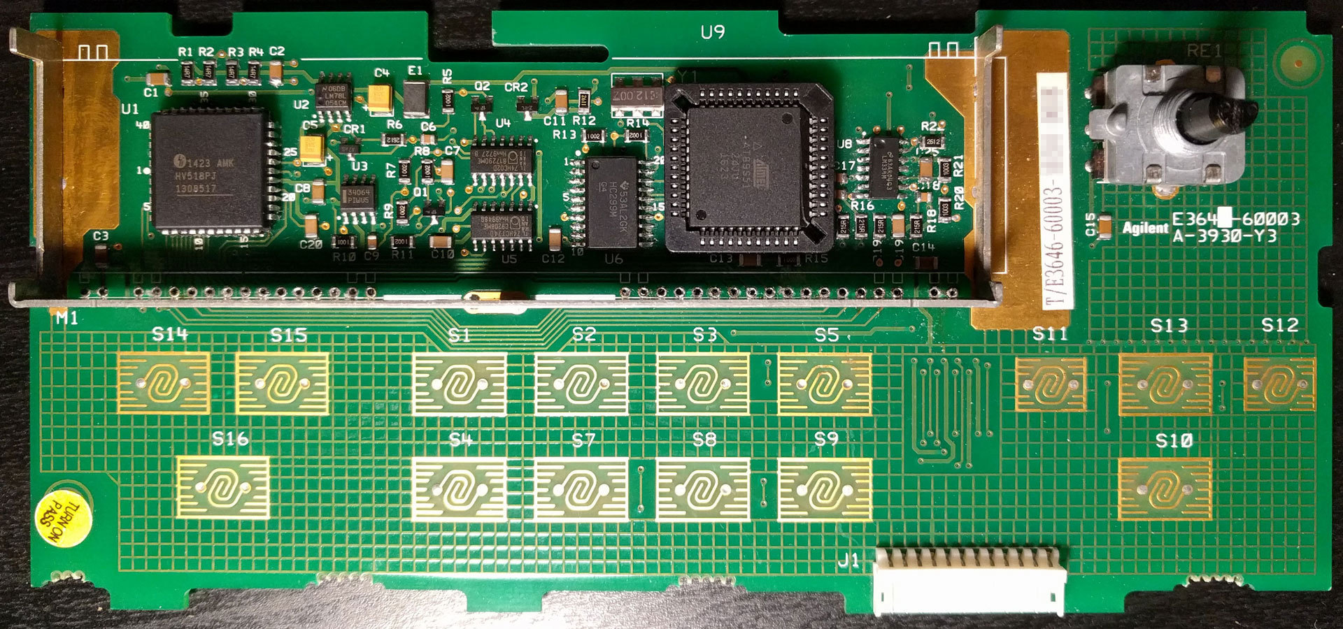
Repaired display board, note changes to U1, U6, and U7 (obscured)
Unfortunately, since the level shifter circuitry is not identical on the input and output, the exact voltage levels for digital low and high differ slightly for each signal. Additionally, the digital logic thresholds on the Saleae Logic differ between various fixed and adjustable voltages depending on the exact model, which I didn’t realize at the time. As a result, I wasted some time replacing good components (diversion #1) before realizing my mistake, switching to the analog sampling mode, and focusing on the microcontroller U7. It turns out that end-of-life 80C51BH model only includes a 4KB factory-programmed read-only memory (ROM) (and not even an ultraviolet erasable programmable read-only memory (UV EPROM), which is on the 87C51). But luckily, even though the 80C51BH doesn’t officially support programming (or lock bits, for that matter, unlike the 87C51), the mask ROM can still be read by a regular programmer. Thus, I was able to use a TL866 programmer to dump the firmware (part number 34401-88804), upload it to KO4BB, reflash it onto a pin-compatible Atmel AT89S51-24JU, and replace U7.
But this didn’t change the symptoms either, so clearly another approach was needed. In order to understand the SPI-like communication protocol between the display and control board, I spent some time disassembling the firmware with IDA Pro, and loaded it into the MCU 8051 emulator. I also compared the firmware binary with the newer version (part number 34401-88813) available at KO4BB, using BinDiff. After identifying each possible response, patching the firmware to send it, and verifying that it was indeed sent over the wire, I became more confident that the problem was elsewhere.
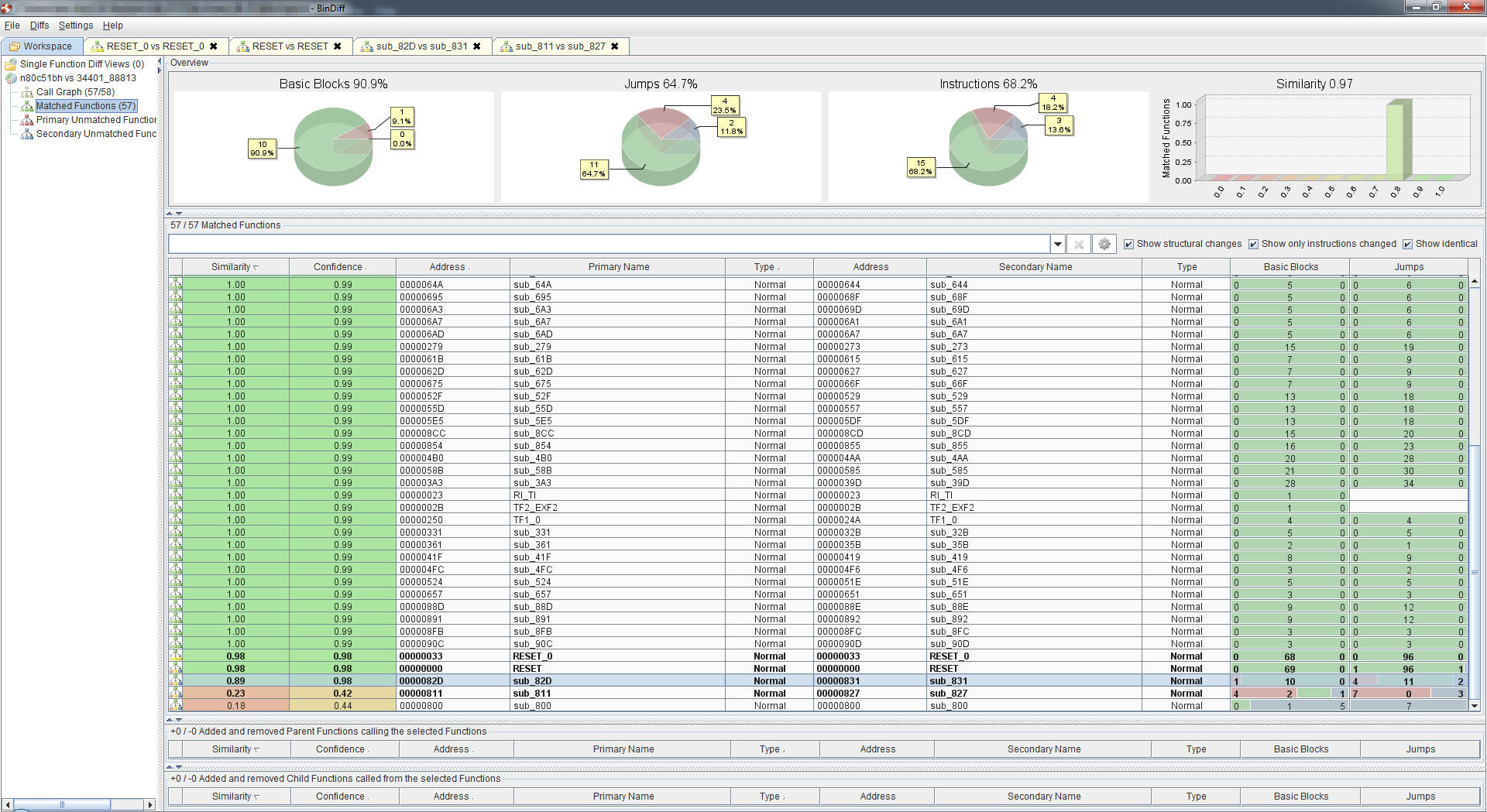
BinDiff analysis of 34401-88804 vs. 34401-88813
Since the FP_DI and FP_SCK signals are clearly received correctly by U7 on the display board, the problem had to lie on the path of the return FP_DO signal. However, I had already verified connectivity through the wire harness and level shifter, suggesting that the fault was with the gate array U16 or its surrounding circuitry, including the auxiliary microcontroller U17. Unfortunately, the gate array U16 is another end-of-life custom part with a factory-programmed mask ROM (part number 1820-8907), which is even more difficult to replace. But, after spending some time searching online, I was able to source a replacement from Utsource, which stocks a lot of end-of-life components, and installed it.
At this point, with the VFD removed, powering on the unit would produce only one long beep, which was an improvement, so I soldered back the VFD, reassembled the unit, and expected it to power on successfully. Alas, that was not to be — the VFD remained blank after startup, and the single long beep was the only change. Cursing my lack of forethought, I disassembled the unit, and attempted to desolder the VFD again. But armed with only a soldering iron and desoldering wick, my second attempt went poorly, and I accidentally broke off a couple of metal leads right at the edge of the glass. This proved to be fatal for the VFD, as I couldn’t even solder wires to the remaining metal stubs, which have very poor solderability and were originally welded to pins.
Gate array U16 being replaced
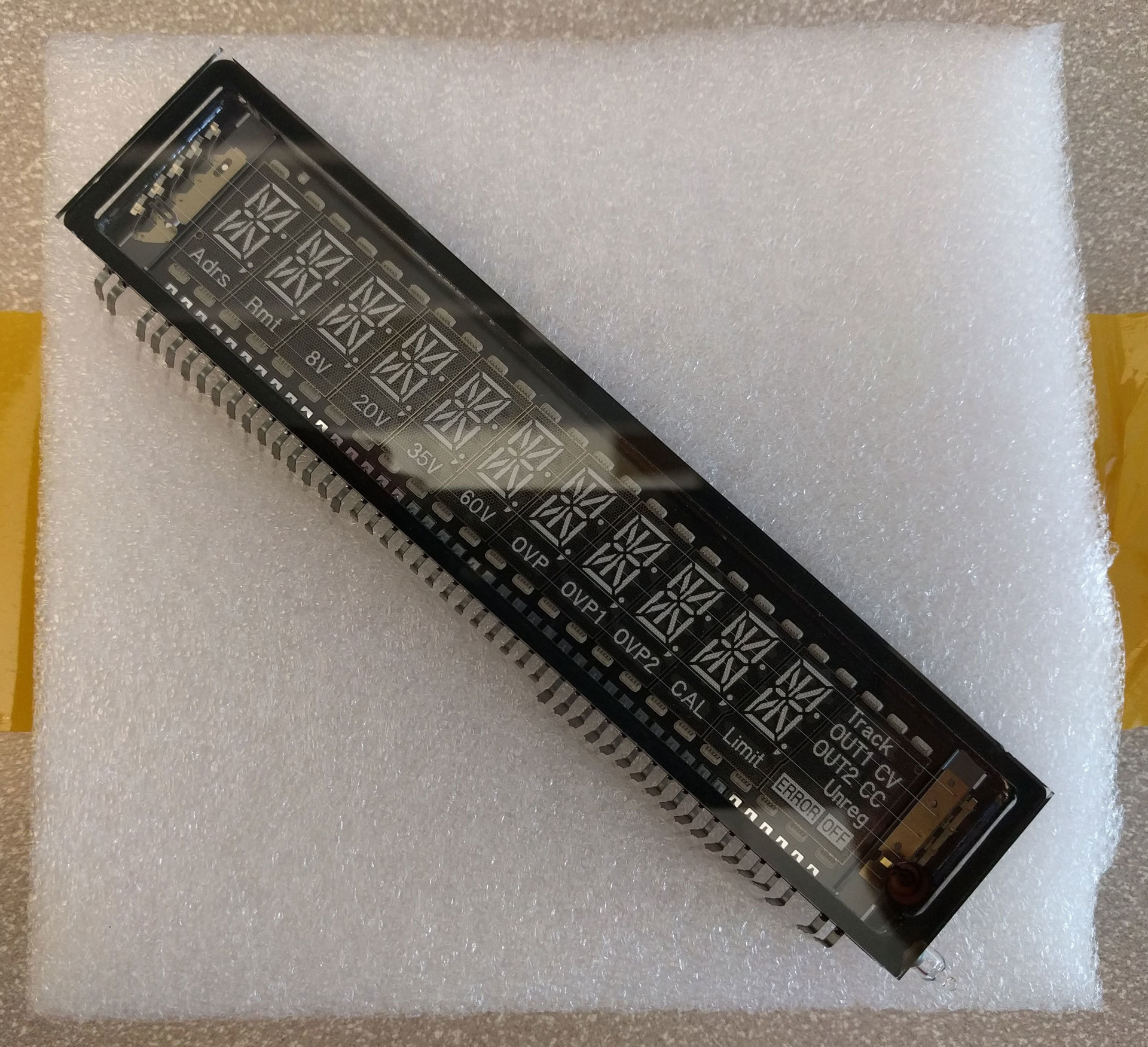
Replacement VFD
In the biggest stroke of luck with this repair, I was able to source a replacement for the Samsung SVI-12MS06 VFD from Shanghai Pufeng Opto Technology in China. And as silver lining, the replacement VFD was much brighter than the original, which was fading from extensive usage. Moving on, after putting a PLCC-32 socket on U7, I probed the display output, which is clocked through another NOR gate (used as a NOT gate) in U4, to the remaining flip-flop in U5, and finally to the VFD driver U1 (Supertex HV518PJ). But despite serial data going in, the high-voltage outputs to the anodes were not engaging, except when the strobe signal was high at startup, suggesting that the shift register or latches were bad. So I replaced this as well, carefully soldered wires to the VFD, and turned on the unit again.
Unfortunately, the symptoms remained the same. Even more confident that the display board was good, but frustrated that I couldn’t find the fault on the control board, I put the repair project on hold, and shelved the unit. But a few months later, I picked up a broken Agilent E3648A power supply, which shares a similar internal design, swapped the control boards, and verified that the fault was somewhere on the control board. Motivated by this confirmation, I replaced a few more components just in case they were bad, including the end-of-life auxiliary microcontroller U17, the end-of-life SRAM U11 (NEC uPD43256BGU-70LL), and the EPROM U12 (AMD AM27C020-150JC) (part number E3646-60023, rev 1.4, available at KO4BB), especially given the existence of a service bulletin describing similar symptoms, but nothing changed (diversion #2).
Later, while examining the control board more closely, I noticed that one of the SOT-23 components CR8 around the analog to digital conversion (ADC) circuitry seemed to be slightly discolored on top (barely visible in preceding photo). Following up in the schematic, I realized that this was not part of the ADC, but actually a reverse-biased zener that supplies +15V to the control board!
At this point, I should mention that my repair was not the first attempt that had been performed on the unit; a previous owner had unsuccessfully replaced a similar bad 2.4V zener diode in the -15V supply on the bottom main board, but I didn’t realize that the control board had its own separate supply.
Incorrect voltage display
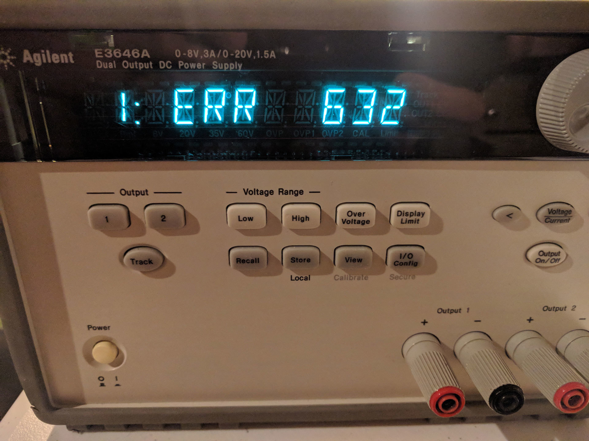
Self-test failure, error 632
Problem #2: +5V Voltage Reference
After replacing this component, the repair became much more straightforward. The unit powered on normally, and would supply regulated power, although the actual output voltage differed significantly from the displayed voltage. This resulted in a self-test failure with error 632, which indicated an issue in the ADC circuitry on the control board. Probing through the circuit, I realized that the precision +5V voltage reference U34 was bad, and temporarily replaced it with a normal +5V voltage regulator to further troubleshoot and confirm.
Problem #3: Overvoltage Supervisor
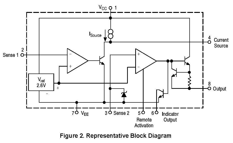
Block diagram of overvoltage supervisor U138
It turns out that the only remaining failure was in the overvoltage protection for output 1, which refused to trigger regardless of the voltage threshold. Cross-referencing the schematic again, I manually applied a digital high to the OVP_TRIP1 signal, which did trigger the overvoltage indicator, suggesting the fault was in the actual overvoltage detection circuitry on the bottom main board. Focusing on the overvoltage supervisor U138 (On Semiconductor MC3423D), the datasheet and block diagram revealed that the first-stage comparator was not triggering, despite the input exceeding the internal 2.6V voltage reference, causing the second-stage comparator to never engage the overvoltage output. Despite being end-of-life, I was able to source another replacement, again from Utsource, and finally completed the repair of this unit.
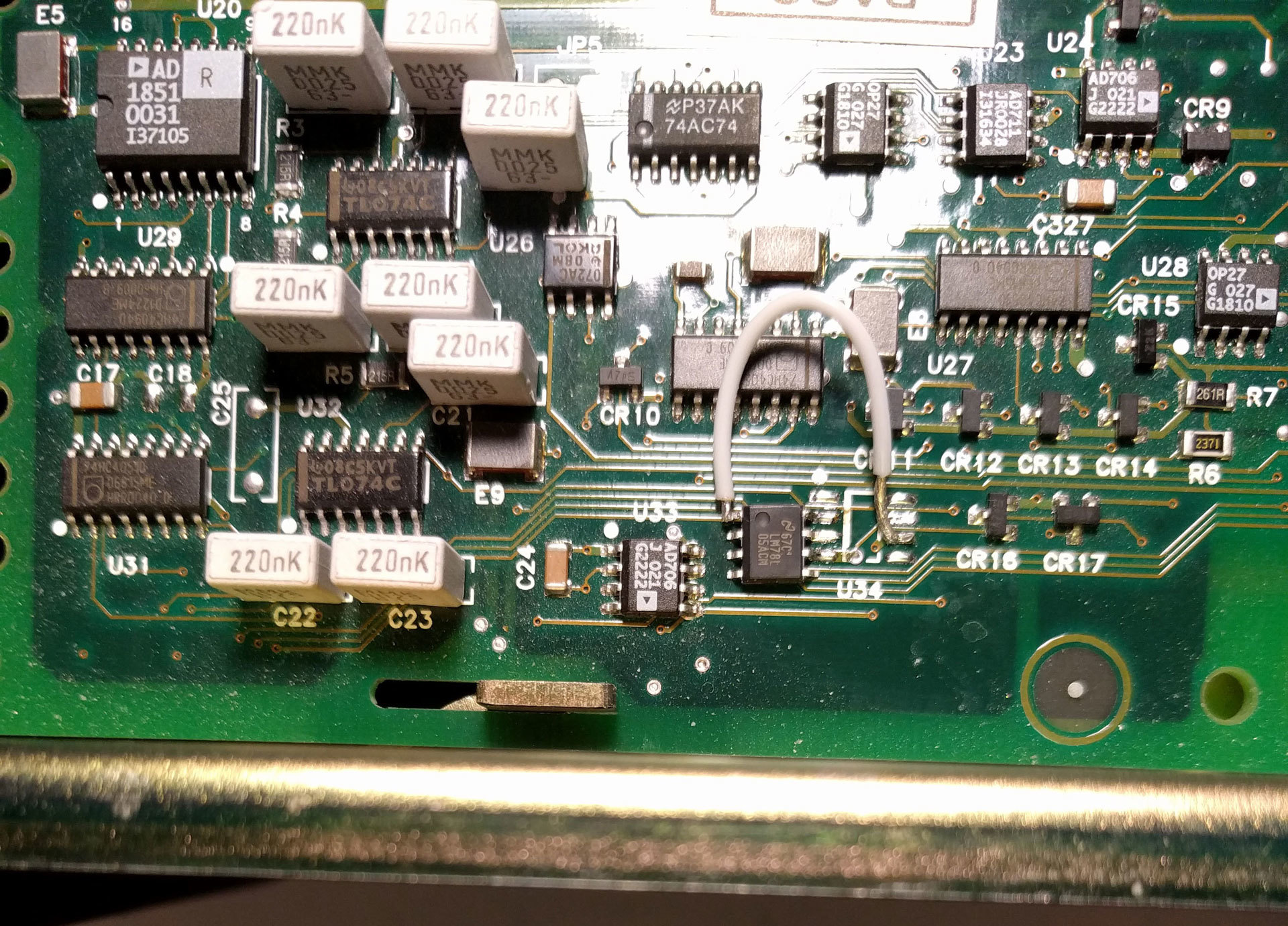
Substitution of a voltage regulator for the +5V voltage reference U34
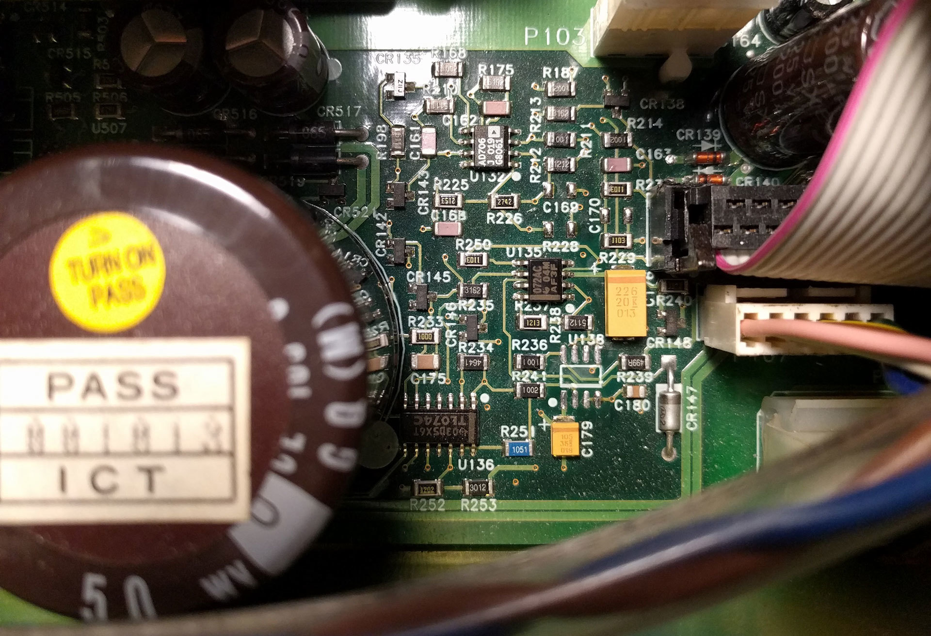
Bad overvoltage supervisor U138 removed
In retrospect, I wasted a lot of time on diversion in both the display and control boards. If I had thoroughly reviewed the entire schematic before starting the repair, I would have probably spent less time, not replaced components that were good, and avoided desoldering the VFD multiple times. Access to better desoldering equipment would have also helped, as it would have reduced the chance of damage during the desoldering process.
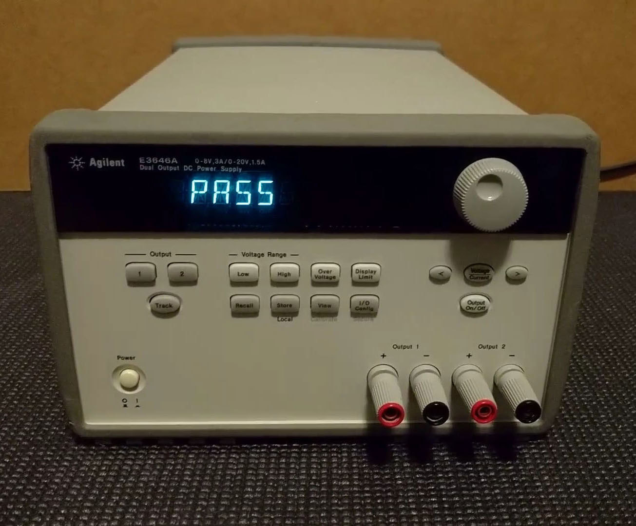
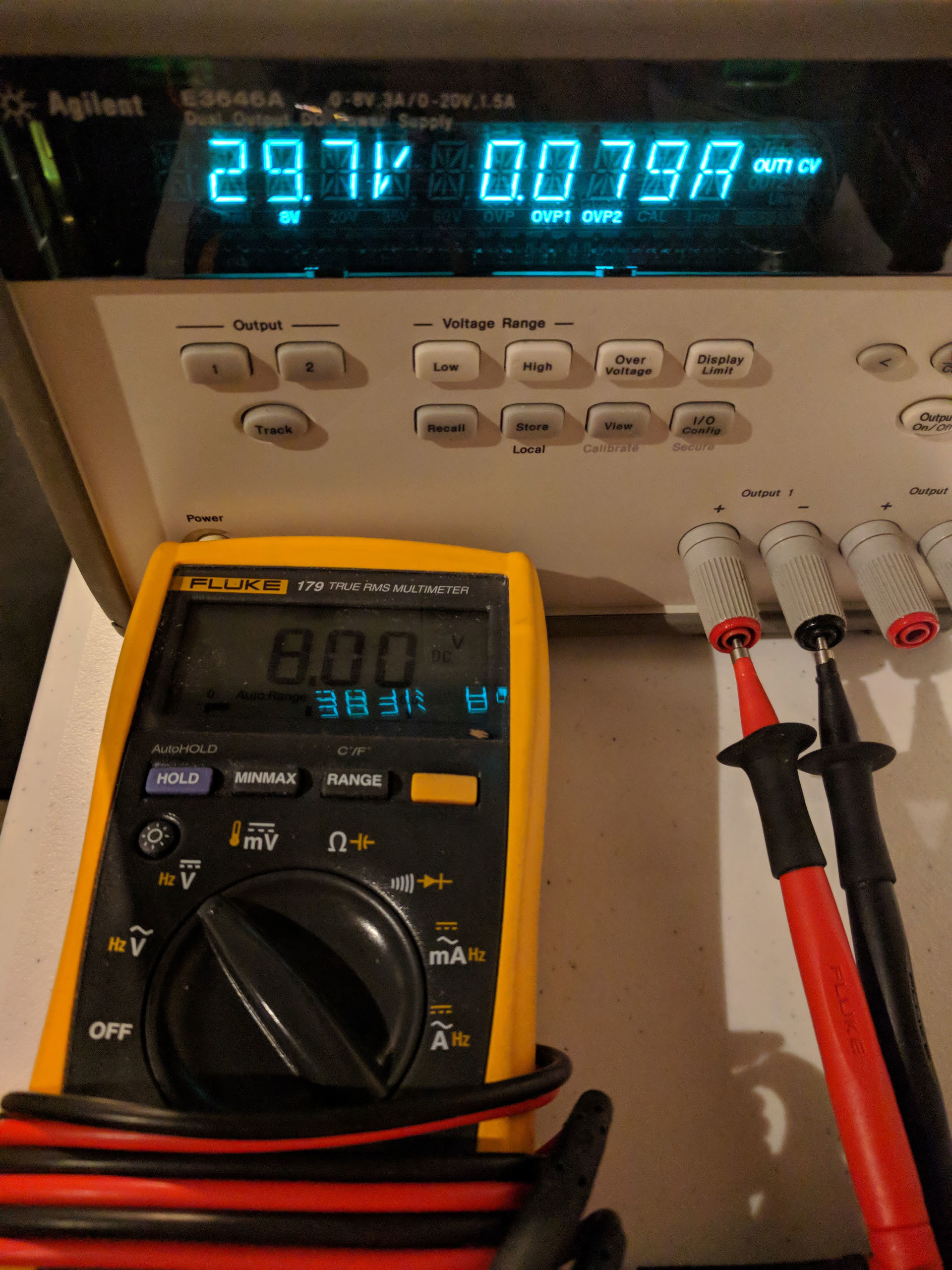
Fully repaired final unit